As electronics continue to shrink in size and increase in functionality, miniaturization has become a key trend in the industry. With devices becoming smaller and more powerful, the need for compact yet reliable circuit board designs is more critical than ever. However, as components get denser, clearance challenges arise, especially in situations where space is limited. To overcome these hurdles, cavity printed circuit boards (PCBs) can be an innovative solution. Instead of relying on thicker or stacked boards, cavity PCBs incorporate cutouts within the layers, optimizing space without compromising performance. Would you like to know more about cavity PCBs?
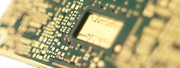
This blog will explore the fundamentals of cavity PCB technology, its applications, benefits, and key considerations during the manufacturing process.
What Is a Cavity PCB?
A cavity PCB has cutouts or holes, known as cavities, extending from the outer copper layer to an inner copper layer but not passing all the way through the board. This technology is used to address specific design challenges, such as embedding components, reducing overall module height, and improving heat dissipation.
Cavity PCBs are particularly effective when used with surface-mount technology (SMT) and allow for more efficient component placement in tight spaces.
Why Use Cavity PCB Technology?
Cavity PCB technology offers several advantages that make it a preferred choice for many engineers and designers. These advantages include:
- Space Optimization: Cavity PCBs make use of previously unused areas, allowing components to fit into dense designs without sacrificing functionality, helping accommodate smaller, more intricate layouts.
- Height Reduction: By placing components at varying levels within the board, cavity PCBs reduce overall height, eliminating the need for taller components or stacked layers.
- Improved Performance: These boards offer better clearance between components, minimizing signal interference and enhancing performance, especially in high-frequency applications.
- Increased Reliability: Reduced component crowding improves airflow and heat dissipation, boosting long-term durability and reducing the risk of mechanical stress or damage.
- Cost Efficiency: Despite the more complex manufacturing process, cavity PCBs reduce space and component height, leading to long-term savings by lowering material costs and assembly times.
Types of Cavity PCBs
When it comes to cavity PCBs, there is no single solution that fits every need. Depending on the specific application and design requirements, different types of cavity PCBs are available.
IPC-Based Types
The IPC standard classifies cavity PCBs based on the amount of copper inside the cavity. Here are the three main types:
- Type 1: No Copper Plating: This is the most basic form of cavity PCB, where the cavity is left with no copper inside. It’s used when the cavity doesn’t require electrical connections or grounding, making it suitable for simple designs.
- Type 2: Copper on Wall or Floor: In this type, copper is applied either to the walls or the floor of the cavity, but not both. It’s often selected when a level of connectivity or grounding is necessary, offering moderate electrical performance.
- Type 3: Copper on Wall and Floor: The most advanced type, copper is applied to both the cavity walls and floor. This provides the best electrical performance and is commonly used in applications requiring thermal management or sensitive signal components.
Layer-based Types
This classification method focuses on the number of PCB layers involved and the placement of the cavity within the board.
- Single-layer Cavity: A straightforward design where the cavity exists on one layer of the PCB. It’s typically used for less complex designs or when only a shallow cavity is required.
- Multi-level PCB Cavity: Cavities that span multiple PCB layers, enabling more complex routing and better support for high-frequency or high-density designs, ideal for advanced applications.
- Embedded Component Cavity: This type fully embeds components inside the cavity, often sealing them in place. Embedded cavity PCBs are used in rugged or highly space-constrained applications, such as wearables or certain industrial devices.
Structure-based Types
Cavity PCBs can also be categorized based on the structure and how the cavity connects to the rest of the board.
- Blind Cavity: A cavity that opens on only one side of the board. It’s commonly used in devices like smartphones, where components need to sit lower without penetrating the other side of the board.
- Buried Cavity: These cavities are fully enclosed within the layers of the board and don’t reach the outer layers. They are ideal for designs that require a sleek, compact form factor, like those in wearables or medical electronics.
- Through Cavity: The cavity goes all the way through the PCB, allowing components to be placed or accessed from both sides of the board. This design is useful for high-density or telecommunications boards where component placement flexibility is essential.
Cavity PCB Manufacturing Process
Manufacturing a cavity PCB is more complex than traditional PCB fabrication, involving specialized equipment and techniques. Here’s an overview of the key steps:
- Design Phase: The process begins by determining the size, shape, and location of cavities within the board. Engineers use advanced design tools to plan the layout, considering component placement, cavity depth, and material properties.
- Layer Stacking: Once the design is finalized, PCB layers are stacked. The cavities are created within inner layers to ensure the board’s structural integrity isn’t compromised.
- Cavity Routing: After stacking, cavities are routed at precise depths using controlled techniques to meet design specifications.
- Assembly and Testing: Next, components are assembled onto the board. SMT testing is performed to ensure the cavities don’t interfere with the board’s functionality, including paste printing and re-flow soldering.
- Final Inspection: Finally, the cavity PCB undergoes inspection to check that all cavities, components, and connections are functioning properly. This ensures the board meets all structural and electrical performance standards.
Applications of Cavity PCBs
Cavity PCBs find applications across various industries where space optimization, signal integrity, and component clearance are crucial. Here are some examples:
- Consumer Electronics: In products like smartphones, laptops, and wearables, where space is limited and high performance is required, cavity PCBs help pack more functionality into smaller devices.
- Telecommunications: PCB cavity for RF applications minimizes signal interference and enhances the performance of communication devices such as antennas and transceivers.
- Automotive: As automotive electronics continue to evolve, cavity PCBs are used in advanced driver-assistance systems (ADAS), infotainment systems, and electric vehicle (EV) components, where compactness and reliability are essential.
- Medical Devices: In medical equipment, cavity PCBs can accommodate sensitive components and ensure that devices are compact while still providing the necessary performance for applications like diagnostics and monitoring.
- Industrial Equipment: For industrial control systems and sensors, cavity PCBs are used to reduce the size of components while maintaining the reliability and functionality of the system.
Optimize Space and Performance with Cavity PCB Technology
HT Global Circuits offers cavity PCBs that reduce component height, optimize space, and enhance performance for compact, high-demand electronics. By incorporating cavities, these PCBs improve layout efficiency and reliability.
Ready to explore how cavity PCB technology can elevate your next project? Send us your design requirements. Our engineers will provide a free DFM report, showing how cavity PCBs can enhance your product’s performance and reliability.