AI workloads are scaling at a pace that most traditional PCB designs were never built to accommodate. From large-scale data center GPU clusters to edge inference modules, the infrastructure supporting AI and high-performance computing (HPC) has placed entirely new demands on how circuit boards are designed, fabricated, and validated.
Conventional laminate structures, standard trace widths, and basic layer counts simply fall short when systems demand ultra-low latency, extreme signal integrity, and sustained thermal output. PCB fabrication process is actively evolving in response. Advanced interconnect strategies, high-density integration techniques, and purpose-built substrate technologies are being introduced to meet these requirements.
In this post covers why Artificial intelligence (AI) and HPC are reshaping fabrication expectations, what the PCB manufacturing process must now deliver, and how industries are applying these advances in practice.
Why AI and HPC Are Reshaping PCB Fabrication Requirements
Artificial intelligence (AI) and HPC systems are no longer incremental upgrades over conventional computing platforms. They operate at fundamentally different performance thresholds, and PCB fabrication and manufacturing processes must align with those demands from the ground up.
Signal Integrity at High Data Rates:
Modern AI accelerators and HPC interconnects operate at extremely high data transfer speeds. Even minor impedance mismatches or signal losses cause data errors that degrade system performance .
Thermal Density Management:
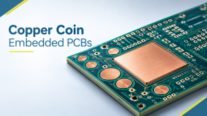
AI processors and HPC chips generate concentrated heat across small die areas. The scale is different from traditional computing: the thermal design power of a single GPU card can reach 600–700 W, and total system power continues to climb. PCBs must support efficient thermal dissipation through embedded copper planes, thermal vias, and heavy-copper power delivery layers to prevent hotspots, component failures, and reduced operational lifespans.
High Layer Count Requirements:
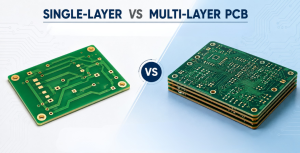
Complex AI hardware integrates hundreds of nets across dense component arrangements. This forces designs to scale layer counts considerably, demanding tighter process control during lamination and drilling operations.
Power Delivery Network Precision:
AI inference and training systems draw heavy, variable power loads. PCBs must deliver clean, stable power across all voltage domains with minimal resistance and inductance throughout the distribution network.
Miniaturization Without Compromise:
Edge AI and compact HPC modules demand smaller form factors. At the same time, these boards must maintain the same electrical performance as their full-scale counterparts, which tightens every fabrication tolerance.
Long-Term Reliability Under Load:
AI and HPC boards often run continuously at near-peak utilization. Boards must maintain electrical and structural integrity across extended thermal cycles, vibration exposure, and high-current operating conditions.
Key PCB Fabrication Requirements for AI and HPC Systems
Getting these boards right goes well beyond standard fabrication. Each design parameter directly influences system reliability, and any compromise during the PCB manufacturing process translates into real-world performance issues.
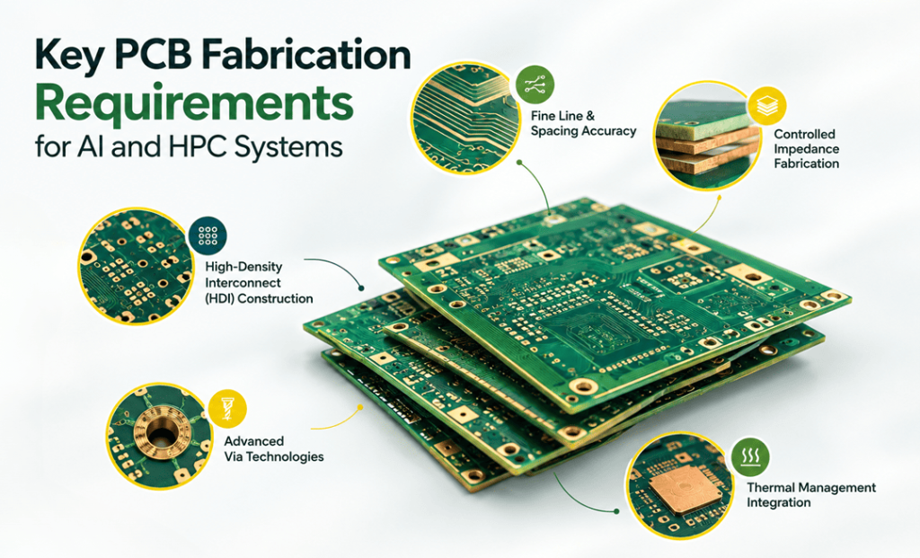
- Fine Line and Spacing Accuracy: AI and HPC PCBs require extremely narrow trace geometries to route signals between dense BGA and flip-chip components. Fabricators must hold tight line and spacing tolerances without yield loss.
- Controlled Impedance Fabrication: High-speed digital interfaces require precisely controlled impedance across every signal layer. This demands accurate dielectric thickness control, consistent copper weights, and validated test protocols at each production stage.
- High-Density Interconnect (HDI) Construction: HDI PCBs with microvias, blind vias, and buried vias allow high component density on compact boards. This is critical for AI modules where interconnect density directly impacts latency and board real estate.
- Advanced Via Technologies: Via-in-pad designs and stacked microvias are standard in high-performance AI boards. These features require precise laser drilling, copper filling, and planarization to maintain electrical continuity and surface flatness.
- Thermal Management Integration: Boards used in AI accelerators often incorporate thermal relief features, embedded copper planes, and direct bonding pads for heat sinks. Each of these must be fabricated to specification for effective system-level cooling.
Emerging PCB Fabrication and Manufacturing Process Technologies Powering the Future
Several fabrication technologies have matured specifically in response to AI and HPC requirements. These are not experimental concepts.
They are production-ready processes already being used across advanced computer platforms.
- Embedded Component Technology: Resistors, capacitors, and even active devices can now be embedded within PCB layers. This shortens interconnect paths, reduces parasitic effects, and frees surface area for additional components.
- Laser Direct Imaging (LDI): LDI replaces traditional photolithography with direct laser patterning. It delivers superior imaging accuracy—typically ±10–15 µm registration compared to ±25–50 µm for traditional photolithography—and is essential for trace/space below 75 µm (3 mil). Modern LDI systems resolve line/space down to 10–25 µm, making them critical for AI boards with sub-3-mil geometries and tight layer-to-layer registration requirements. .
- Any-Layer HDI Fabrication: Any-Layer HDI (ELIC) Fabrication: Any-layer HDI, formally called ELIC (Every Layer Interconnect), uses exclusively copper-filled stacked microvias with no mechanical through-holes anywhere in the board. This allows direct copper connections between any two layers and supports BGA pitches down to 0.4 mm and below. The trade-off is significant: any-layer construction requires 5–7+ sequential lamination cycles and costs 4–7× a conventional multilayer board. It is justified only when routing density is the binding constraint. .
- Advanced Surface Finishes: Advanced Surface Finishes: ENIG, ENEPIG, and immersion silver all provide flat, solderable surfaces suitable for fine-pitch assembly. However, for high-speed AI boards, the electrical trade-off matters. Above roughly 1 GHz, the nickel in ENIG and ENEPIG is the loss mechanism—its relative permeability is in the hundreds, and its conductivity is about a quarter of copper’s. Immersion silver has no nickel and delivers the lowest insertion loss above 1 GHz, making it the preferred finish for 25G/56G+ interfaces. ENEPIG adds a palladium barrier that eliminates black pad and supports gold ball bonding, but the nickel loss penalty remains. The choice is not purely about solderability—it is a signal integrity decision.
- Automated Optical and X-Ray Inspection: Advanced inspection systems can detect sub-micron defects across complex multilayer constructions. For AI and HPC boards, these tools are essential to verify internal layer quality before final assembly.
Challenges in Manufacturing AI and HPC PCBs
PCB manufacturing process for Artificial intelligence (AI) and HPC is technically demanding. The combination of high layer counts, fine features, and strict electrical requirements creates a set of challenges as follows:
- Registration Accuracy Across Many Layers: Registration Accuracy Across Many Layers: On boards with 20+ layers, maintaining layer-to-layer registration within ±25 µm (1 mil) is technically demanding. Misalignment directly threatens annular ring integrity—critical for IPC Class 3, which requires a minimum 1 mil annular ring with no breakout—and causes via-to-pad misregistration that changes impedance and degrades eye diagrams at high data rates. The challenge compounds with each lamination cycle: a 32-layer PCB boards may require 5–7 sequential laminations, each adding an opportunity for registration drift.
- Copper Distribution and Stress Management: Uneven copper distribution across inner layers creates mechanical stress during lamination. This can cause warpage, delamination, and dimensional instability, all of which affect downstream assembly and reliability.
- Drilling Precision for Microvias: Laser drilling microvias to tight diameter and depth tolerances is technically demanding. Inconsistencies in via geometry directly affect resistance values and signal integrity in high-speed AI circuits.
- Material Behavior Under Process Conditions: High-performance laminates behave differently under heat and pressure compared to standard FR4. Fabricators must adjust processing parameters carefully to avoid resin starvation, layer shifting, or Tg-related failures.
- Yield Management on Complex Designs: High-complexity AI and HPC boards have more opportunities for defects per unit area. Managing yield without inflating costs requires tightly controlled processes, experienced operators, and thorough inspection protocols.
- Meeting Increasingly Tight Electrical Specs: AI systems demand impedance accuracy and insertion loss performance that leaves very little room for variation. Achieving and consistently repeating these results across production volumes requires advanced process control.
How Advanced Manufacturing Practices Address These Challenges
The challenges described above are addressable. Fabricators that invest in the right equipment, processes, and engineering capabilities can consistently deliver boards that meet even the most demanding AI and HPC specifications. Here are the advanced manufacturing practices that help address the challenges in AI and HPC PCB fabrication:
- Design for Manufacturability (DFM) Reviews: Early-stage DFM analysis identifies potential fabrication issues before production begins. Addressing these at the design phase reduces costly rework and improves first-pass yield on complex AI board designs.
- Impedance Modeling and Pre-Production Testing: Fabricators use simulation tools and controlled test coupons to verify impedance performance before committing full panels to production. This prevents expensive failures on high-value AI and HPC assemblies.
- Advanced Lamination Process Control: Tightly controlled lamination cycles with precise time, temperature, and pressure management reduce registration errors and copper stress. This is especially important on boards with more than a standard layer count.
- Statistical Process Control (SPC) in Production: Real-time SPC monitoring flags process deviations as they occur. For AI and HPC fabrication, this means consistent output quality across production runs without relying on end-of-line inspection alone.
- Skilled Engineering Support Across the Build Cycle: Complex AI boards often require engineering involvement at multiple stages, from stackup selection through final inspection. This level of support differentiates capable fabricators from commodity manufacturers.
- Traceability and Quality Documentation: Full traceability from raw material to finished board is expected on high-reliability AI and HPC projects. Thorough documentation supports root cause analysis, regulatory compliance, and customer confidence.
Partner with a Fabricator Built for High-Performance Demands
Artificial intelligence (AI) and HPC are setting new benchmarks for what PCBs must deliver. Every layer, via, and trace carries more responsibility than it did in previous-generation designs.
HT Global Circuits offers advanced PCB fabrication services built to meet these exact requirements, from HDI and high-layer-count boards to controlled impedance and thermal management constructions.
For more details or customization queries, visit our website today at www.htglobalcircuits.com and get a tailored solution for your next AI or HPC project.
Frequently Asked Questions (FAQs)
Heavier copper weights reduce I²R losses in power planes and thermal vias, improving heat transfer away from high-dissipation components. The thermal argument is quantitative: copper conducts heat at roughly 385 W/m·K, compared to about 0.3 W/m·K for FR-4—a difference of more than 1,000×. This is why 2 oz and 3 oz copper are common in AI accelerator PDNs, and why thermal vias plated with heavy copper are effective at moving heat into internal planes or the opposite side of the board. The trade-off is fabrication complexity: heavy copper requires adjusted etch compensation, longer plating cycles, and tighter lamination control.
Any-layer HDI allows vias to connect any two layers directly rather than just adjacent ones. This provides routing flexibility critical for complex AI processor boards that would otherwise require excessive layer counts to achieve the same interconnect density.
Even small panel-to-panel impedance variation causes signal reflection and timing inconsistencies. The manufacturing data is revealing: positional variation alone can create a 2–3% impedance spread across a single panel, and standard-process boards typically show a standard deviation of around 3.5% in impedance distribution. For AI interfaces operating at PCIe Gen 4 and above, this spread is unacceptable. Tight-tolerance impedance control (±5% or better) requires stackup simulation using measured Dk from the actual material lot, etch compensation calibrated to the specific geometry, and TDR verification on every panel—processes that add 15–30% to board cost but are non-negotiable at 16 GT/s and above.
Yes. AI-based monitoring systems can detect process anomalies in real time during imaging, drilling, and lamination. This reduces defect propagation across a production run and improves overall yield on complex, high-value AI and HPC board designs.