Thermal management is one of the biggest challenges in the design and manufacturing of high-power printed circuit boards (PCBs). As modern electronics continue to demand higher performance, devices such as power regulators, Metal-Oxide-Semiconductor Field-Effect Transistor (MOSFETs), and Insulated Gate Bipolar Transistors (IGBTs) generate significant heat during operation. Managing this heat is crucial because excessive temperatures can lead to component failure, reduced efficiency, and even system downtime.
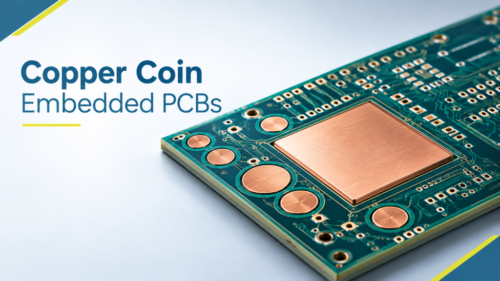
This is where the embedded copper coin PCB comes into play. A copper coin PCB integrates solid copper coins within the PCB layers to directly dissipate heat from high-power components. This innovative solution enhances thermal performance and supports multilayer designs, offering engineers a powerful way to manage heat in demanding applications. Would you like to know more about why we use copper coin embedded PCBs, how they outperform traditional thermal solutions, and the specific industries that benefit from their advanced thermal management capabilities? Continue reading to know.
Why Use Copper Coin Embedded PCBs?
Below are the key reasons why using copper coin embedded PCBs is beneficial in modern electronics
- Superior Heat Dissipation: The primary advantage of PCB with copper coin technology is exceptional heat dissipation capability. Traditional thermal via arrays create a heat path through drilled holes, but these are limited by small diameter and thermal resistance of surrounding dielectric materials. A copper coin embedded PCB provides a direct, high-mass thermal pathway with significantly lower thermal resistance. The solid copper coin enables rapid heat transfer from the component junction to the board’s backside or mounting surfaces. The large thermal mass also helps with heat spreading, distributing energy across a wider area, and reducing peak temperatures.
- Supports Multilayer Designs: Typical layer counts range from 4 to 6 layers, with 6-layer constructions common for balancing thermal performance, routing, and cost. 2-layer and 8-layer constructions are available as special capabilities. This multilayer capability is essential for modern electronics requiring intricate signal routing, multiple power planes, controlled impedance traces, and dense component placement. The embedded copper coin occupies a defined footprint but doesn’t interfere with routing on other layers. This provides designers with complete flexibility for routing high-speed differential pairs, implementing proper ground planes, and designing power distribution networks, all while ensuring optimal thermal performance.
- Improved Reliability for Power Devices: Thermal cycling is a leading cause of failure in power electronics. Excessive heat accelerates semiconductor degradation and can lead to catastrophic failure. By maintaining lower junction temperatures, copper coin PCBs significantly improve the reliability and lifespan of power devices. For MOSFETs and IGBTs operating at high currents, even a 10°C reduction in junction temperature can dramatically extend operational life. This improved thermal performance translates directly to higher system reliability and reduced failure rates in demanding applications.
Copper Coin PCB vs Other Thermal Solutions
When comparing embedded copper coin PCBs to other thermal solutions, such as MCPCBs, it’s important to consider the advantages and limitations of each. Below is a comparison of copper coin PCBs to other thermal solutions.
| Feature | Copper Coin PCB | MCPCB (Metal Core PCB) | Thermal Vias |
| Thermal Management | Direct heat path from component to copper mass, ensuring efficient heat dissipation. | Uses a metal core (e.g., aluminum or copper) for heat dissipation, but is limited to a lower layer count. | Thermal vias help heat escape to lower layers, but become insufficient when power density exceeds approximately 5–10W in a concentrated area, at which point a copper coin provides a more effective thermal path |
| Design Flexibility | Supports complex multilayer designs, offering more routing options while maintaining thermal control. | Most commonly single or double-layer, though multilayer designs (up to 8+ layers) are possible but more complex and costly. | Mostly used in simpler PCBs with few layers, limiting routing flexibility. |
| Reliability | Improves component reliability by providing stable thermal management for high-power devices (e.g., MOSFETs, IGBTs). | Less reliable for complex or high-power systems, as heat dissipation is less effective. | Thermal vias may not always ensure consistent temperature control, leading to potential reliability issues. |
How Copper Coin PCBs Are Manufactured (High-Level)
The copper coin PCB manufacturing process involves several precision steps to ensure the copper coins are properly embedded into the PCB structure.
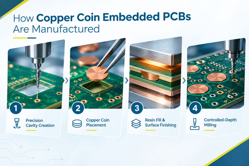
Here’s a high-level overview of the process:
- Precision Cavity Creation: Manufacturing begins with machining a cavity in the FR-4 core. The copper coin size shall be 0.075mm (single side) smaller than the FR-4 window opening to allow for proper fitting and resin flow during lamination.
- Copper Coin Placement: : The copper coin is placed into the cavity. The copper coin inlay thickness must be carefully measured to ±1 mil, and the height tolerance of FR-4 vs. copper coin inlay must be less than 30µm for proper planarity.
- Lamination and Planarity Control: During lamination, epoxy resin flows into gaps, creating mechanical and thermal bonds. Planarity is controlled to within 30µm, and copper coin dimension tolerance is controlled to X/Y axis ±50µm.
- Resin Fill and Surface Finishing: Remaining gaps are filled for structural integrity, then the board proceeds through standard PCB processing, such as drilling, plating, etching, and surface finishing.
- Controlled-Depth Milling: For copper coin inlay boards requiring blind routing, controlled-depth milling is used to maintain precise depth control and avoid damaging the copper coin or inner layers.
Stack-Up Considerations for Copper Coin PCBs
Proper stack-up design is essential for optimizing the thermal and electrical performance of copper coin PCBs.. Typical layer counts range from 4 to 6 layers , with 6-layer constructions common for balancing thermal performance, routing, and cost. 2-layer and 8-layer constructions are available as special capabilities.
For an ideal stack-up, position the copper coin directly beneath the component’s thermal pad to ensure efficient heat dissipation.
In a typical 6-layer stackup (1.5mm thick), the coin might span L2 to L5, measuring 20mm × 10mm × 1.5mm. Copper coin sizes range from 5mm × 5mm to 80mm × 80mm. Copper coin thicknesses range from 1.0mm to 2.5mm. Copper coins are available in cylinder or cube/cuboid shapes (with radius) and must be solid without holes.

Key clearance requirements:
- Cu coin to inner layer circuit: minimum 0.30mm
- Cu coin to plated through-holes (PTH): minimum 0.40mm
- Cu coin to non-plated holes (NPTH): minimum 0.30mm
- Cu coin to board outline: minimum 0.70mm

Sample: 3L Copper Coin Inlay Board with Depth Control Blind Routing

Typical Applications of Copper Coin Embedded PCBs
Copper coin embedded PCBs are commonly used in applications where high thermal performance and multilayer designs are required. Some typical applications include:
- Power Electronics: Copper coin PCBs are ideal for power devices, including power regulators and converters, that generate substantial heat during operation.
- Automotive Power Modules: These PCBs are used in electric vehicles (EVs) and hybrid vehicles (HEVs) for efficient power conversion and heat management.
- Industrial Motor Drives: Copper coin PCBs help manage heat in industrial motor control systems, improving reliability and performance.
- High-Current DC/DC Converters: These power devices benefit from copper coin PCBs to ensure stable operation under high-power conditions.
- LED Power Control Boards: Copper coin technology helps dissipate heat in LED drivers and controllers, extending the life of the components.
When Should You Choose a Copper Coin PCB?
Use this decision checklist to determine if a copper coin embedded PCB is the right solution for your application:
- Is the power density too high? If your component dissipates more than 5-10W in a concentrated area and thermal vias cannot maintain safe junction temperatures, a copper coin may be necessary.
- Is multilayer routing required? If your design needs 4 or more layers for signal routing, power distribution, and ground planes, copper coins provide better thermal performance than thermal vias while maintaining routing flexibility that MCPCBs cannot offer.
- Is there a localized hotspot? Copper coins excel at managing localized high-power components. If your thermal challenge is concentrated under specific power devices rather than distributed across the entire board, targeted copper coin placement is highly effective.
Ready to optimize your high-power PCB design with copper coin technology? Contact HT Global Circuits today to discuss your thermal management requirements. Request a quote to explore how embedded copper coin solutions can solve your toughest thermal challenges.