Most conversations around PCB design tend to focus on schematic capture or component selection. However, printed circuit board routing is equally critical, as it defines how electrical signals travel across the board from one point to another. Well-executed routing preserves signal integrity, manages current flow, and supports effective heat distribution. This becomes especially important in high-speed or mixed-signal designs, where even minor routing decisions can impact overall performance.
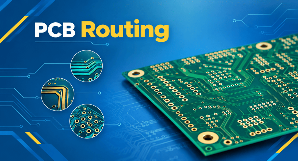
Poor routing choices, such as tight spacing, uneven copper, or sharp trace angles, can lead to issues like shorts, opens, and inconsistent etching. These problems often surface during testing, resulting in additional revision cycles, increased costs, and delays in time-to-market. Needless to say, effective PCB routing is where design intent aligns with manufacturing capability.
This PCB routing tutorial explains what PCB routing is, highlights common pitfalls, and outlines best practices that lead to reliable and manufacturable boards.
What is PCB Routing?
The PCB routing process comprises creating electrical connections between components on a printed circuit board using conductive traces. It translates the schematic into physical pathways that carry signals and power across the board.
HT Global Circuits supports routing for a full range of PCB types, including Rigid PCB, Flexible PCB, Rigid-Flex PCB, HDI, and High-Frequency Boards. Our engineering team provides DFM feedback during the routing stage to catch potential manufacturing issues before fabrication begins.
- PCB routing is not an isolated step. It sits between design planning and physical production, translating schematic intent into a manufacturable layout.
- Component Placement: Components are strategically positioned based on functionality, signal flow, thermal considerations, and mechanical constraints. Good placement reduces routing complexity.
- Routing: Electrical connections are established using copper traces, vias, and planes. This stage ensures that signals travel efficiently and without interference.
- Fabrication and Assembly: The routed design is manufactured into a physical PCB, where copper layers are etched, drilled, and assembled with components.
- Each stage influences the next. Poor placement can complicate routing, while ineffective routing can create manufacturing challenges or performance issues.
- Effective PCB routing bridges the gap between electrical design and manufacturable output, ensuring that the final board performs reliably under real-world conditions.
Manual Routing vs. Auto-Routing: What Engineers Should Know
Most PCB design tools include built-in auto-routing capabilities. They offer speed and convenience, and new engineers may be prompted to use auto-routing tools, especially on boards with high component density.

However, experienced engineers tend to rely heavily on manual routing, especially for production designs. Here is the comparison between auto routing and manual routing.
| Aspect | Auto Routing | Manual Routing |
| Basic Approach | Automated trace routing using built-in algorithms | Engineer-controlled routing with full design intent |
| Speed & Convenience | Fast and easy; useful for quick results | Slower; requires time and expertise |
| Awareness of Electrical Behavior | No real awareness of signal integrity, thermal effects, or fabrication nuances | Full awareness; engineers optimize for signal behavior, thermal load, and manufacturability |
| Routing Quality | Generic paths focused on connectivity | Optimized paths tailored to performance and reliability |
| Via Usage | Often excessive and unnecessary vias | Controlled and minimized via usage |
| Trace Paths | Can be awkward, inefficient, and non-intuitive | Clean, logical, and easy to follow |
| Spacing & Clearances | Uses minimum rule limits; may be too tight for comfort | Engineers apply practical margins beyond minimum rules |
| Layout Readability | Can appear chaotic and cluttered | Clean and readable with clear signal flow |
| Handling High-Density Designs | Can attempt dense routing, but may create congestion issues | Better control for complex, high-density layouts |
| Production Readiness | Requires significant manual cleanup | Typically ready for fabrication when completed properly |
| Design Optimization | Limited optimization capability | High level of optimization possible |
| Debugging & Review | Harder to review and debug | Easier to analyze and troubleshoot |
| Reliability for Final Design | Risky if used alone | Preferred approach for production-quality PCBs |
| Best Use Cases | Feasibility checks, congestion detection, and early-stage exploration | Final production designs and high-reliability boards |
Factors to Consider for Correct PCB Routing
There are various parameters to consider to ensure effective PCB routing, which will lead to a flawless design.
- PCB Trace Width: Electrical and Manufacturing Considerations: The following considerations are essential when defining trace widths:
- Impact on Electrical Performance: Trace width directly affects current-carrying capacity, voltage drop, and overall circuit reliability. Selecting an appropriate width is essential to ensure stable operation.
- Current Carrying Capacity: The relationship between current and trace width is direct. Higher current requires wider traces to safely conduct electricity without excessive resistance.
- Thermal Considerations: Narrow traces have higher resistance, which leads to increased heat generation under load. Excessive heat can degrade the trace and reduce long-term reliability.
- Copper Thickness: Trace performance is also influenced by copper weight (thickness). Thicker copper allows higher current capacity without requiring excessive trace width.
- Standards and Design Guidelines: Industry standards such as IPC-2221 and IPC-2152 provide established guidelines for determining minimum trace width based on current, temperature rise, and copper thickness.
- Manufacturing Constraints: While narrow traces may help in dense layouts, manufacturers generally prefer wider traces for better yield, consistency, and reliability across production batches.
- Practical Design Approach: A practical approach is to size traces based on electrical requirements and include a safety margin wherever possible. Minimum trace widths should be used only in space-constrained areas rather than as a default across the design.
- Trace Spacing: Preventing Shorts and Manufacturing Defects: The following considerations should be evaluated when determining appropriate spacing:
- Electrical Isolation Requirements: Adequate spacing ensures proper isolation between signals, which is essential in high-voltage and high-speed designs. Insufficient clearance can lead to arcing, leakage currents, or signal interference such as crosstalk.
- Dependence on Voltage and Application Standards: Required spacing is influenced by voltage differentials, operating environment, and applicable industry standards. Higher voltages typically demand greater clearance to maintain safety and performance.
- Manufacturing Tolerances: Fabrication processes such as etching can introduce slight variations in trace dimensions. If spacing is too tight, these variations can cause adjacent traces to merge, resulting in short circuits.
- Impact on Yield and Reliability: Tight spacing increases the likelihood of defects during fabrication and assembly, including issues with solder mask application. This can reduce production yield and affect long-term reliability.
- Cost and Process Implications: Designs that operate at minimum spacing limits may require tighter process controls and advanced fabrication capabilities, which can increase manufacturing cost and lead time.
- Practical Design Approach: Spacing should be defined based on both electrical requirements and manufacturing capabilities. Avoid using minimum clearances unless necessary, and include reasonable margins to improve yield and consistency.
- Avoiding Right-Angle Traces: Electrical and Etching Risks: Here are the points to consider to eliminate electrical and etching risks.
- Formation of Acid Traps: Right-angle trace bends have been a point of debate in PCB design for years. While they may look clean in the layout, right-angle traces may lead to the formation of acid traps during etching. Sharp corners can trap etching chemicals, leading to uneven material removal. However, modern PCB fabrication processes, including alkaline and photo-activated etching, have significantly reduced this concern. For most current designs, acid traps are no longer a primary manufacturing risk. This can create defects in the trace only in legacy or improperly controlled etching processes.
- Signal Reflections: The electrical argument against them is that sharp corners create a small but real impedance discontinuity, which can theoretically cause signal reflections. While this may not matter for low-speed designs, it is only a practical concern in extremely high-speed designs, typically above 10 GHz, where the discontinuity length becomes a significant fraction of the signal wavelength. Empirical testing and simulation have shown that for most high-speed digital designs operating below 10 GHz, the effect of a 90° bend on return loss and insertion loss is negligible.
- Ideal Bends: It is recommended to use 45° bends or smooth curved traces. These shapes are easier to manufacture for some fabricators and can provide more consistent electrical performance in very high-frequency designs. However, for most designs, the choice of bend geometry has minimal impact on electrical performance and should be balanced against layout density and routing efficiency.
PCB Routing Best Practices for Manufacturability
Following PCB routing guidelines reduces the back-and-forth between design and fabrication and improves manufacturability and electrical performance.
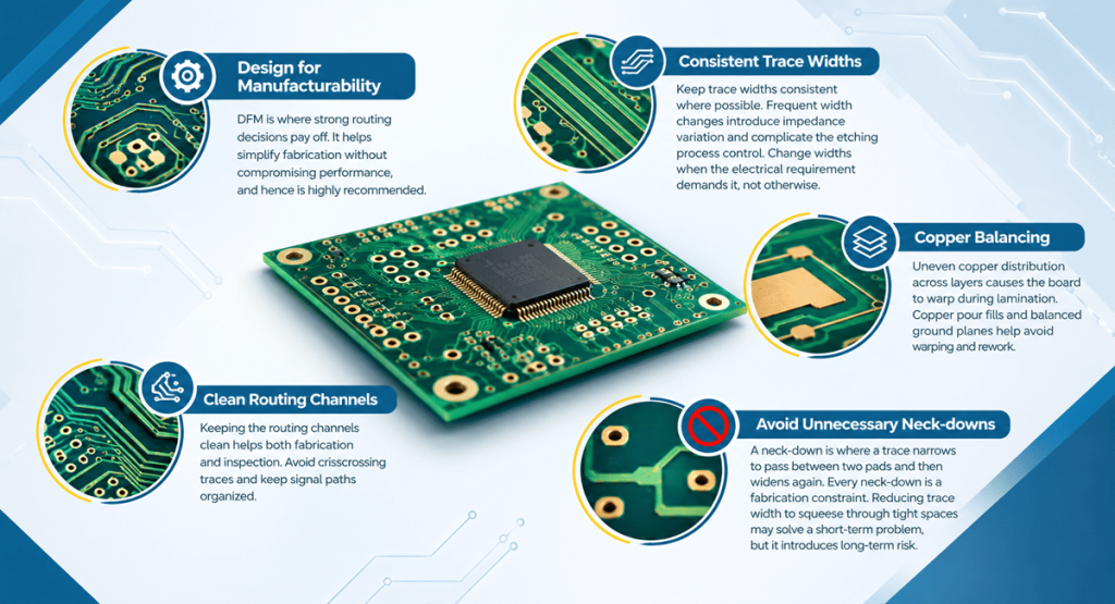
- Design for Manufacturability: DFM is where strong routing decisions pay off. It helps simplify fabrication without compromising performance, and hence is highly recommended.
- Consistent Trace Widths: Keep trace widths consistent where possible. Frequent width changes introduce impedance variation and complicate the etching process control. Change widths when the electrical requirement demands it, not otherwise.
- Copper Balancing: Uneven copper distribution across layers causes the board to warp during lamination. Copper pour fills and balanced ground planes help avoid warping and rework.
- Clean Routing Channels: Keeping the routing channels clean helps both fabrication and inspection. Avoid crisscrossing traces and keep signal paths organized.
- Avoid Unnecessary Neck-downs: A neck-down is where a trace narrows to pass between two pads and then widens again. Every neck-down is a fabrication constraint. Reducing trace width to squeeze through tight spaces may solve a short-term problem, but it introduces long-term risk.
- At HT Global Circuits, we support controlled impedance routing with ±10% tolerance, minimum trace widths and spacing down to 3 mil, and up to 44 layers for complex designs. Our DFM review process helps designers optimize routing for manufacturability before production.
How Good Routing Improves Fabrication Outcomes
The connection between routing quality and fabrication outcomes is direct and measurable. The following outcomes highlight the importance of well-executed routing:
- Higher Production Yield: Conservative trace widths, adequate spacing, and proper bend geometries improve manufacturability and reduce the likelihood of defects.
- Reduced Defects per Panel: Cleaner routing minimizes issues such as shorts, opens, and etching inconsistencies, leading to a higher number of usable boards per production run.
- Fewer Design Revisions: Routing that aligns with Design for Manufacturability (DFM) guidelines reduces the need for redesign cycles after initial fabrication feedback.
- Improved Production Efficiency: Well-defined geometries and standard-compliant layouts allow fabrication teams to proceed without delays caused by ambiguous or borderline design features.
- HT Global Circuits’ engineering team reviews routing for manufacturability as part of our standard DFM process, helping to reduce revision cycles and improve first-pass yield.
Design with Fabrication in Mind
PCB routing is not just a finishing step. It is a critical part of the design process that influences performance, manufacturability, and reliability. Early discipline in routing leads to smoother manufacturing later. It reduces risk, saves time, and improves product quality.
Partnering with the right Bare PCB Boards service provider is equally critical to achieving consistent and reliable results.

Also Read: